Trustworthy · Efficient · Professional
A professional source PCB manufacturer.
Feitian focuses on the R&D and production of high-multilayer, high-frequency & high-speed, heavy-copper, optical-module and IC-substrate PCBs — and provides PCB design & layout services.
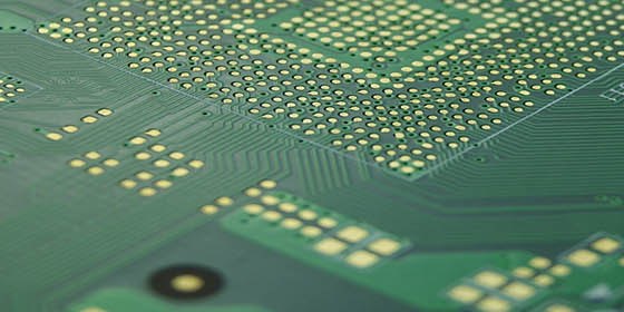
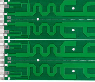
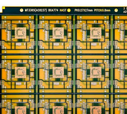
Nine product families. One factory floor.
Commodity boards, high-frequency laminates and IC substrates all run under one roof in Wuping — nine families, one inspection standard, one process engineering team. A mixed BOM stays with one vendor instead of being split across several.
 High-Frequency PCBRogers · PTFE · Cavity boards · RO4350B · RO58805G base stations · Radar · Microwave
 High-Speed PCBHigh-speed digital · Impedance-controlledServers · Switches
 Multilayer PCBMultilayer · Blind/buried via · AnylayerComplex high-density designs
 Heavy Copper PCBHeavy copper · High-current boardsPower supplies · Automotive
 Optical Module PCBOptical-module PCBsData-centre optical comms
 HDI & IC SubstrateIC Substrate · IC test boardsChip packaging
 Hybrid Laminate PCBHigh-frequency + FR-4 hybrid stackupsPerformance-cost balance
 Metal Base PCBAluminium-base · Copper-baseHigh heat-dissipation scenarios
 Standard PCBDouble-sided · 4-layer conventional FR-4General-purpose needs
From file to shipment in five steps.
Upload your Gerber
RS-274X, drill files or ODB++. Zip is fine, up to 200 MB.
DFM review
An engineer checks stackup, clearances and impedance. Within 24 hours.
Quote and confirm
Price, lead time and tooling in one document. No hidden engineering fee.
Fabrication
Lot tracking from lamination to final inspection, with photo updates on request.
Test and ship
Electrical test, AOI, impedance coupons. DHL or FedEx, tracked.
15,000 m², owned. Not a trading desk with a website.
Most suppliers you find on page one are brokers. We laminate, drill, plate and test across three buildings in Wuping, Fujian — at the junction of Fujian, Guangdong and Jiangxi, with daily freight lines across China.
- ✓200+ skilled staffA stable management team backed by experienced process engineers.
- ✓LDI imaging, VCP plating, AOI + AVI inspectionIn-house lab: network analyser, impedance, ion-contamination and PIM testing.
- ✓50,000 m² monthly output, 1,200 modelsHigh-mix, low-to-mid volume. No minimum on prototypes.
Send the file. Get a real answer.
Upload a Gerber and we will come back within 24 hours with the DFM issues, a price and a lead time. If your design is not a fit for our process, we will say so.